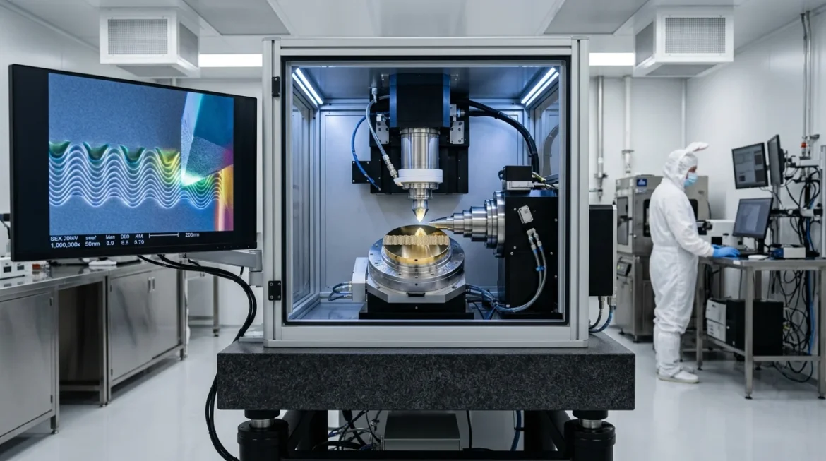
The science of structuring and removing material with sub-100-nanometer features is known as nano machining. In fact, conventional methods rely on macroscopic shearing forces. In contrast, atomic-scale processing manipulates matter atom by atom.
For example, a single strand of human DNA measures roughly 2.5 nanometers across. Meanwhile, a standard sheet of paper is about 100,000 nanometers thick. Therefore, classical continuum mechanics does not apply at this scale. Instead, tool edge radius and crystal lattice orientation dictate cut quality. As a result, manufacturers achieve flawless optical finishes without manual polishing.
Nano Machining vs Micro Machining vs Conventional CNC
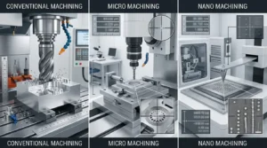
Understanding the difference between nanomachining and micromachining is essential for engineering teams. Specifically, each manufacturing tier serves different dimensional requirements and tolerance levels.
| Machining Level | Dimensional Scale | Typical Tolerances | Surface Roughness (Ra) | Common Tooling / Energy Source | Primary Applications |
| Conventional CNC | $> 1\text{ mm}$ | $\pm 10\text{ to } 50\text{ }\mu\text{m}$ | $0.8\text{ to } 3.2\text{ }\mu\text{m}$ | Tungsten carbide, HSS endmills | Automotive engine blocks, enclosures |
| Micro Machining | $1\text{ }\mu\text{m} – 1\text{ mm}$ | $\pm 1\text{ to } 5\text{ }\mu\text{m}$ | $0.1\text{ to } 0.4\text{ }\mu\text{m}$ | Micro-endmills, wire EDM, lasers | Watch gears, fuel injectors, stents |
| Nano Machining | $0.1 – 100\text{ nm}$ | $\pm 0.001\text{ to } 0.1\text{ }\mu\text{m}$ | $< 0.001 – 0.005\text{ }\mu\text{m}$ | Monocrystalline diamond, FIB, lasers | Photonic chips, contact lens molds |
First, conventional CNC operates in millimeters. Second, micro machining produces parts in the micrometer range. Finally, nano machining delivers sub-micron tolerances for high-end photonics and quantum sensors.
Core Technologies and Types of Nano Machining
Engineers categorize modern nanoscale manufacturing into three core approaches: mechanical tooling, focused beams, and chemical replication.
Mechanical Ultra-Precision Machining
Mechanical processes rely on physical contact between a single-crystal diamond tool and the workpiece.
-
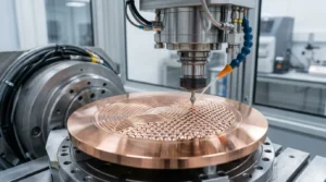
Single Point Diamond Turning (SPDT): SPDT shears non-ferrous metals along molecular slip planes. Consequently, it achieves surface roughness values under 2 nanometers without post-polishing.
-
Ultra-Precision Diamond Milling: In addition, diamond milling handles non-rotational freeform optics. It uses high-speed air spindles to carve micro-grooves and lens arrays accurately.
Beam-Based and Direct-Write Systems
Beam systems operate without physical contact. Therefore, they prevent mechanical stress on delicate substrates.
-
Focused Ion Beam (FIB) Machining: A stream of gallium or xenon ions strikes the substrate. As a result, physical sputtering ejects atoms to create custom nanoscale patterns.
-
Electron Beam Lithography (EBL): EBL uses focused electron beams to expose resist layers. Thus, it remains the primary method for writing semiconductor photomasks.
Ultrafast Laser Processing and Functional Texturing
Femtosecond laser pulses last only $10^{-15}$ seconds. Because the pulse is so fast, heat does not spread into surrounding material. This cold ablation creates burr-free micro-features.
Furthermore, ultrafast pulses create Laser-Induced Periodic Surface Structures (LIPSS). By adjusting laser polarization, engineers form self-assembled nanoscale ripples. Consequently, these patterned surfaces gain superhydrophobic and antibacterial properties.
Chemical, Abrasive, and Replication Methods
-
Atomic Layer Etching (ALE): ALE removes a single atomic layer per cycle using gas-surface reactions.
-
Chemical Mechanical Planarization (CMP): In contrast, CMP combines chemical slurries and abrasive pads to flatten silicon wafers.
-
Nanoimprint Lithography (NIL): NIL stamps nanoscale patterns into soft polymers. Therefore, it lowers production costs compared to slow beam-based lithography.
Critical Machine Architecture and Environmental Controls
Standard factory floors cannot support nanoscale production. For this reason, facilities install specialized machine bases inside cleanrooms.
-
Aerostatic and Hydrostatic Spindles: Porous graphite air bearings float rotating machine shafts. Consequently, radial runout stays below 12.5 nanometers.
-
Vibration Damping Foundations: Machines sit on active pneumatic mounts and solid granite beds. Thus, ambient building vibrations never reach the cutting tool.
-
Extreme Thermal Stabilization: Machine enclosures circulate chilled fluid to control temperatures within $\pm 0.01^\circ\text{C}$. In fact, a single degree of temperature drift expands aluminum by over 2 micrometers. Therefore, strict thermal control is essential to preserve sub-micron accuracy.
Material Compatibility: From Noble Metals to Brittle Ceramics
Material composition directly determines tool longevity and cutting behavior.
-
Non-Ferrous Metals (Al, Cu, Ni, Au, Ag): These alloys machine cleanly with diamond tools. Moreover, they deliver mirror finishes with minimal tool wear.
-
Ferrous Alloys and Hardened Steels: Diamond tools degrade quickly on steel due to chemical wear. Instead, technicians use ultrasonic-assisted tooling or ultrafast lasers.
-
Semiconductor Substrates (Silicon, GaAs, GaN): These brittle materials require planar etching or FIB milling to prevent surface cracking.
-
Optical Glasses and Ceramics (Sapphire, Fused Silica): These substrates require ductile-mode grinding. Specifically, shallow cuts allow plastic shear before fractures form.
-
Polymers (PMMA, Polycarbonate): Because polymers are ductile, they work well for micro-optics and nanoimprint replication.
Design for Nanomanufacturability (DFNM) and Sub-Surface Damage
Engineers must follow specific design guidelines when planning nanoscale parts.
-
Aspect Ratio Limits: Tall, thin features often collapse during wet cleaning rinses. Therefore, designers add small fillets to support tall structures.
-
Mitigating Sub-Surface Damage (SSD): Heavy cutting loads cause micro-cracks under brittle surfaces. Consequently, operators take very shallow finishing passes to protect optical clarity.
-
Crystallographic Orientation: In single-crystal substrates, cutting resistance changes with grain direction. For this reason, tool paths must align with natural cleavage planes.
Quality Assurance and Nanoscale Metrology
Standard mechanical gauges cannot measure nanoscale features. Instead, quality teams rely on non-destructive metrology systems.
-
Atomic Force Microscopy (AFM): An ultra-sharp probe tip scans the surface profile. As a result, AFM measures roughness and step heights down to angstroms.
-
Field Emission Scanning Electron Microscopy (FE-SEM): FE-SEM uses high-energy electron beams to capture high-magnification images of sub-10-nanometer features.
-
Optical and Laser Interferometry: This non-contact method measures light wave interference patterns. Therefore, it verifies overall lens curvature across large areas in seconds.
Industrial Applications and Production Economics
Nanoscale manufacturing supports growth across multiple high-tech industries.
-
Advanced Photonics: AR/VR lenses, laser mirrors, and optical filters.
-
Semiconductor Fabrication: EUV photomasks and sub-2-nanometer transistor gates.
-
Biomedical Implants: Microfluidic diagnostic chips and cell-guiding scaffolds.
-
Quantum Devices: Silicon qubits and atomic-scale resonators.
From an economic perspective, fabrication methods differ in cost and speed. Direct-write tools like FIB and EBL offer immense design freedom. However, their slow cycle times make mass production expensive.
In contrast, high-volume production relies on replication. Manufacturers use diamond turning to carve a master mold. Then, they replicate thousands of parts using nanoimprint lithography and precision micro-molding.
Frequently Asked Questions
What is the minimum tolerance achievable in nano machining operations?
Ultra-precision diamond lathes and beam tools achieve tolerances between $\pm 0.001\text{ }\mu\text{m}$ ($1\text{ nm}$) and $\pm 0.05\text{ }\mu\text{m}$ ($50\text{ nm}$). However, results depend on material stability and temperature control.
Why cannot standard CNC endmills achieve nano-level precision?
Standard CNC machines suffer from mechanical bearing runout and frame vibration. In addition, carbide cutting edges are too dull to shear material cleanly at the atomic scale.
How does Single Point Diamond Turning produce optical mirror finishes without polishing?
SPDT uses a monocrystalline diamond tool with a cutting edge under 100 nanometers. Furthermore, it runs on an air-bearing spindle to shear clean crystal planes without leaving tool marks.
What is the difference between top-down and bottom-up nanoscale manufacturing?
Top-down manufacturing carves nanoscale features out of larger bulk materials using diamond tools and ion beams. In contrast, bottom-up manufacturing synthesizes molecules chemically through vapor deposition and self-assembly.